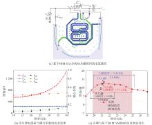
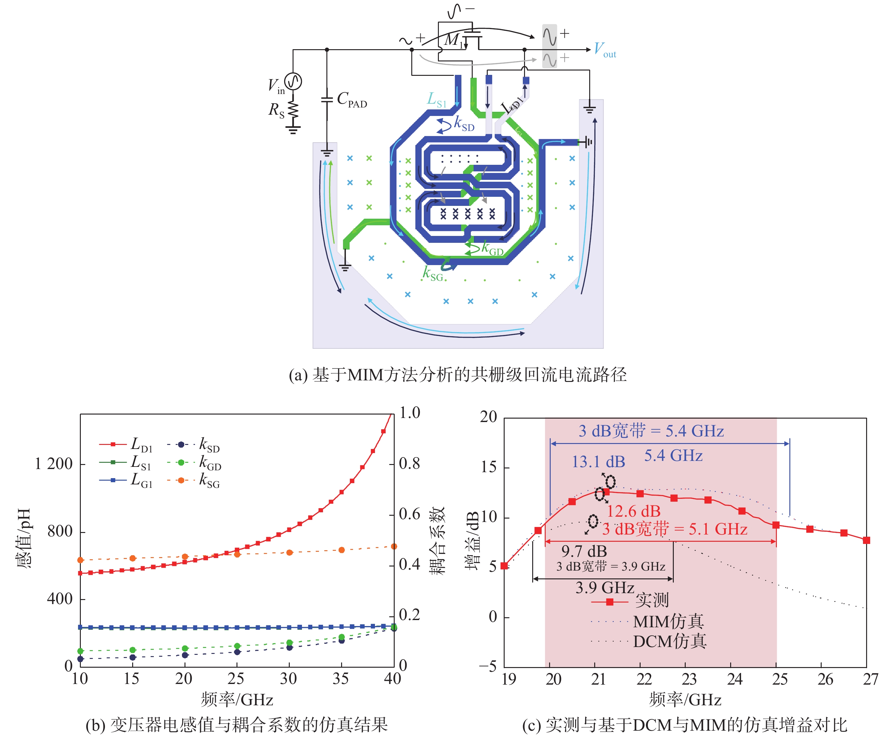
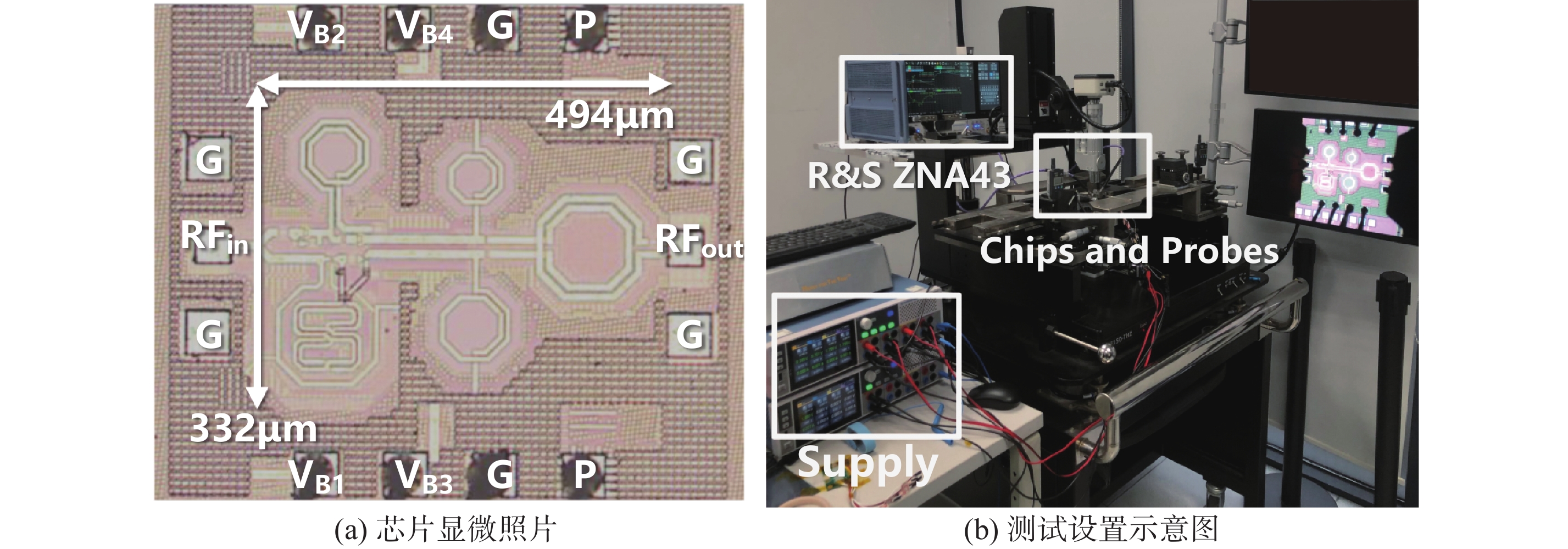
| 1 |
TABARANI F, BOCCIA L, PURTOVA T, et al.. 0.25-μm BiCMOS system-on-chip for K-/Ka-band satellite communication transmit–receive active phased arrays. IEEE Transactions on Microwave Theory and Techniques, 2018, 66 (5): 2325- 2339.
|
| 2 |
LOW K K W, KANAR T, ZIHIR S, et al.. A 17.7–20.2-GHz 1024-element K-band SATCOM phased-array receiver with 8.1-dB/K G/T, ±70° beam scanning, and high transmit isolation. IEEE Transactions on Microwave Theory and Techniques, 2022, 70 (3): 1769- 1778.
|
| 3 |
FU X, YOU D, WANG X L, et al.. A low-power 256-element ka-band CMOS phased-array receiver with on-chip distributed radiation sensors for small satellite constellations. IEEE Journal of Solid-State Circuits, 2023, 58 (12): 3380- 3395.
|
| 4 |
LU H, LI N Y, GAO H Y, et al. A K-band 4-element 8-beam phased-array receiver with hybrid vector interpolation and impedance-adapted multibeam combining techniques for satellite communications [C]// 2024 IEEE Radio Frequency Integrated Circuits Symposium (RFIC). IEEE, 2024: 167-170.
|
| 5 |
FU X, YOU D, WANG Y, et al.. A low-power radiation-hardened ka-band CMOS phased-array receiver for small satellite constellation. IEEE Journal of Solid-State Circuits, 2024, 59 (2): 349- 363.
|
| 6 |
FRIESICKE C, FEUERSCHUTZ P, QUAY R, et al. A 40 dBm AlGaN/GaN HEMT power amplifier MMIC for SatCom applications at K-band [C]// 2016 IEEE MTT-S International Microwave Symposium (IMS). IEEE, 2016: 1-4.
|
| 7 |
ALJUHANI A H, REBEIZ G M. A 12.5 mW packaged K-band CMOS SOI LNA with 1.5 dB NF [C]// 2019 IEEE MTT-S International Microwave Symposium (IMS). IEEE, 2019: 156-159.
|
| 8 |
ZHANG J, ZHAO D, and YOU X. A 20 GHz 1.9-mW LNA using gm-boost and current-reuse techniques in 65-nm CMOS for satellite communications[J]. IEEE Journal of Solid-State Circuits, 2020, 55(10): 2714-2723.
|
| 9 |
ZHANG H, FAN X H, SINENCIO E S.. A low-power, linearized, ultra-wideband LNA design technique. IEEE Journal of Solid-State Circuits, 2009, 44 (2): 320- 330.
|
| 10 |
SHIM Y, KIM C W, LEE J, et al. Design of full band UWB common-gate LNA [J]. IEEE Microwave and Wireless Components Letters, 2007, 17(10): 721-723.
|
| 11 |
LO Y T, KIANG J F.. Design of wideband LNAs using parallel-to-series resonant matching network between common-gate and common-source stages. IEEE Transactions on Microwave Theory and Techniques, 2011, 59 (9): 2285- 2294.
|
| 12 |
MONDAL S, SINGH R, HUSSEIN A I, et al.. A 25–30 GHz fully-connected hybrid beamforming receiver for MIMO communication. IEEE Journal of Solid-State Circuits, 2018, 53 (5): 1275- 1287.
|
| 13 |
LEE J, HONG S.. A 21–41-GHz common-gate LNA with TLT matching networks in 28-nm FDSOI CMOS. IEEE Microwave and Wireless Components Letters, 2022, 32 (9): 1051- 1054.
|
| 14 |
SHAEFFER D K, LEE T H.. A 1.5-V, 1.5-GHz CMOS low noise amplifier. IEEE Journal of Solid-State Circuits, 1997, 32 (5): 745- 759.
|
| 15 |
NGUYEN T K, KIM C H, IHM G J, et al.. CMOS low-noise amplifier design optimization techniques. IEEE Transactions on Microwave Theory and Techniques, 2004, 52 (5): 1433- 1442.
|
| 16 |
CUI B L, LONG J R.. A 1.7-dB minimum NF, 22–32-GHz low-noise feedback amplifier with multistage noise matching in 22-nm FD-SOI CMOS. IEEE Journal of Solid-State Circuits, 2020, 55 (5): 1239- 1248.
|
| 17 |
BHAGAVATULA V, TAGHIVAND M, RUDELL J C.. A compact 77% fractional bandwidth CMOS band-pass distributed amplifier with mirror-symmetric Norton transforms. IEEE Journal of Solid-State Circuits, 2015, 50 (5): 1085- 1093.
|
| 18 |
LIAO C F, LIU S I.. A broadband noise-canceling CMOS LNA for 3.1–10.6-GHz UWB receivers. IEEE Journal of Solid-State Circuits, 2007, 42 (2): 329- 339.
|
| 19 |
BLAAKMEER S C, KLUMPERINK E A M, LEENAERTS D M W, et al.. Wideband Balun-LNA with simultaneous output balancing, noise-canceling and distortion-canceling. IEEE Journal of Solid-State Circuits, 2008, 43 (6): 1341- 1350.
|
| 20 |
LIU Z, BOON C C, LI C, et al. A 0.0078 mm2 3.4 mW wideband positive-feedback-based noise-cancelling LNA in 28-nm CMOS exploiting Gm boosting [C]// IEEE International Solid-State Circuits Conference. 2022: 1-3.
|
| 21 |
YU H H, CHEN Y, BOON C C, et al.. A 0.096-mm2 1–20-GHz triple-path noise- canceling common-gate common-source LNA with dual complementary pMOS–nMOS configuration. IEEE Transactions on Microwave Theory and Techniques, 2020, 68 (1): 144- 159.
|
| 22 |
DENG Z X, ZHOU J, QIAN H J, et al.. A 22.9–38.2-GHz dual-path noise-canceling LNA with 2.65–4.62-dB NF in 28-nm CMOS. IEEE Journal of Solid-State Circuits, 2021, 56 (11): 3348- 3359.
|
| 23 |
ALI M H M, LER C L, RUSTAGI S C, et al. The impact of electromagnetic coupling of guard ring metal lines on the performance of on-chip spiral inductor in silicon CMOS [C]// 2nd Asia Symposium on Quality Electronic Design (ASQED). IEEE, 2010: 285-288.
|
| 24 |
KANAR T, REBEIZ G M.. X- and K-band SiGe HBT LNAs with 1.2- and 2.2-dB mean noise figures. IEEE Transactions on Microwave Theory and Techniques, 2014, 62 (10): 2381- 2389.
|
| 25 |
KODAK U, REBEIZ G M.. A 5G 28-GHz common-leg T/R front-end in 45-nm CMOS SOI with 3.7-dB NF and −30-dBc EVM with 64-QAM/500-MBaud modulation. IEEE Transactions on Microwave Theory and Techniques, 2019, 67 (1): 318- 331.
|
| 26 |
KONG S, LEE H D, JANG S, et al. A 28-GHz CMOS LNA with stability-enhanced gm-boosting technique using transformers [C]// 2019 IEEE Radio Frequency Integrated Circuits Symposium (RFIC). IEEE, 2019: 7-10.
|
| 27 |
SHAHEEN R A, RAHKONEN T, PÄRSSINEN A.. Millimeter-wave frequency reconfigurable low noise amplifiers for 5G. IEEE Transactions on Circuits and Systems II: Express Briefs, 2021, 68 (2): 642- 646.
|
| 28 |
KOBAL E, SIRIBURANON T, CHEN X, et al.. A Gm-boosting technique for millimeter-wave low-noise amplifiers in 28-nm triple-well bulk CMOS using floating resistor in body biasing. IEEE Transactions on Circuits and Systems I: Regular Papers, 2022, 69 (12): 5007- 5017.
|
| 29 |
CHENG D P, CHEN X, CHEN Q, et al.. A reconfigurable LNA with compact magnetic-capacitive coupling transformer networks for 5G 28-/ 39-GHz applications. IEEE Microwave and Wireless Technology Letters, 2024, 34 (7): 915- 918.
|
| 30 |
KIM J H, SON J T, LIM J T, et al.. Ultralow noise figure and broadband CMOS LNA with three-winding transformer and large transistor. IEEE Transactions on Microwave Theory and Techniques, 2024, 72 (5): 2734- 2744.
|
 )
)
 中文核心期刊