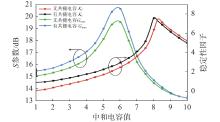
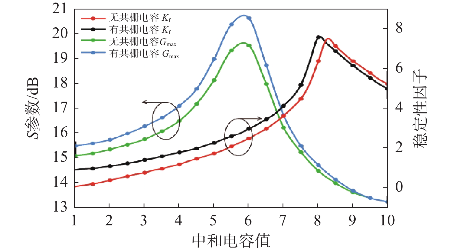
| 1 |
BRUCCOLERI F, KLUMPERINK E A M, NAUTA B.. Wide-band CMOS low-noise amplifier exploiting thermal noise canceling. IEEE Journal of Solid-State Circuits, 2004, 39 (2): 275- 282.
|
| 2 |
YU H H, CHEN Y, BOON C C, et al.. A 0.096-mm2 1-20 GHz triple-path noise- canceling common-gate common-source LNA with dual complementary pMOS–nMOS configuration. IEEE Transactions on Microwave Theory and Techniques, 2020, 68 (1): 144- 159.
|
| 3 |
HUYNH P B T, KIM J H, YUN T Y.. Dual-resistive feedback wideband LNA for noise cancellation and robust linearization. IEEE Transactions on Microwave Theory and Techniques, 2022, 70 (4): 2224- 2235.
|
| 4 |
LIU Z, BOON C C, LI C Y, et al. A 0.0078 mm2 3.4 mW wideband positive-feedback-based noise-cancelling LNA in 28 nm CMOS exploiting Gm boosting [C]// 2022 IEEE International Solid- State Circuits Conference (ISSCC). IEEE, 2022: 1-3.
|
| 5 |
MOEZZI M, SHARIF BAKHTIAR M.. Wideband LNA using active inductor with multiple feed-forward noise reduction paths. IEEE Transactions on Microwave Theory and Techniques, 2012, 60 (4): 1069- 1078.
|
| 6 |
LIAO C F, LIU S I.. A broadband noise-canceling CMOS LNA for 3.1-10.6 GHz UWB receivers. IEEE Journal of Solid-State Circuits, 2007, 42 (2): 329- 339.
|
| 7 |
GUO B Q, CHEN J, LI L, et al.. A wideband noise-canceling CMOS LNA with enhanced linearity by using complementary nMOS and pMOS configurations. IEEE Journal of Solid-State Circuits, 2017, 52 (5): 1331- 1344.
|
| 8 |
VIGILANTE M, REYNAERT P. 20.10 A 68.1-to-96.4 GHz variable-gain low-noise amplifier in 28 nm CMOS [C]// 2016 IEEE International Solid-State Circuits Conference (ISSCC). IEEE, 2016: 360-362.
|
| 9 |
MONDAL S, SINGH R, HUSSEIN A I, et al.. A 25-30 GHz fully-connected hybrid beamforming receiver for MIMO communication. IEEE Journal of Solid-State Circuits, 2018, 53 (5): 1275- 1287.
|
| 10 |
ZOU L F, ZHAO K J, FANG Z H, et al. A 74.8-88.8 GHz wideband CMOS LNA achieving + 4.73 dBm OP1dB and 6.39 dB minimum NF [C]// 2023 IEEE/MTT-S International Microwave Symposium. IEEE, 2023: 60-63.
|
| 11 |
LEE J, HONG S.. A 21–41-GHz common-gate LNA with TLT matching networks in 28-nm FDSOI CMOS. IEEE Microwave and Wireless Components Letters, 2022, 32 (9): 1051- 1054.
|
| 12 |
SATO M, TAKAHASHI T, HIROSE T.. 68–110-GHz-band low-noise amplifier using current reuse topology. IEEE Transactions on Microwave Theory and Techniques, 2010, 58 (7): 1910- 1916.
|
| 13 |
LI X Y, SHEKHAR S, ALLSTOT D J.. Gm-boosted common-gate LNA and differential colpitts VCO/QVCO in 0.18-μm CMOS. IEEE Journal of Solid-State Circuits, 2005, 40 (12): 2609- 2619.
|
| 14 |
YANG K T, BOON C C, FENG G Y, et al. 6.7 A 1.75dB-NF 25mW 5GHz transformer-based noise-cancelling CMOS receiver front-end [C]// 2021 IEEE International Solid- State Circuits Conference (ISSCC). IEEE, 2021: 102-104.
|
| 15 |
SHIN W, CALLENDER S, PELLERANO S, et al. A compact 75 GHz LNA with 20 dB gain and 4 dB noise figure in 22 nm FinFET CMOS technology [C]// 2018 IEEE Radio Frequency Integrated Circuits Symposium (RFIC). IEEE, 2018: 284-287.
|
| 16 |
KONG S, LEE H D, LEE M S, et al.. A V-band current-reused LNA with a double-transformer-coupling technique. IEEE Microwave and Wireless Components Letters, 2016, 26 (11): 942- 944.
|
| 17 |
BIERBUESSE D, NEGRA R. 60 GHz variable gain & linearity enhancement LNA in 65 nm CMOS [C]// 2020 IEEE Radio Frequency Integrated Circuits Symposium (RFIC). IEEE, 2020: 163-166.
|
| 18 |
YUNG-PEI L, BAI W T, HUANG T W, et al. A 70-to-110 GHz 28-nm CMOS low noise amplifier with 6.1-dB NF minimum using differential noise optimization [C]// 2024 IEEE International Symposium on Circuits and Systems (ISCAS). IEEE, 2024: 1-4.
|
| 19 |
HAN C X, ZHOU J, LUO X.. A 70–86-GHz deep-noise-canceling LNA with dual-stage noise cancellation using asymmetric compensation transformer and 4-to-1 hybrid-phase combiner. IEEE Journal of Solid-State Circuits, 2025, 60 (3): 1030- 1042.
|
| 20 |
HAN A R, LI Q X, ZHOU J, et al. A 50-68 GHz IF absorptive receiver with 8-GHz IF-bandwidth supporting 16-channel carrier-aggregation and 12Gbps-64QAM modulation for 5G NR FR2-2 application [C]// 2025 IEEE Radio Frequency Integrated Circuits Symposium (RFIC). IEEE, 2025: 131-134.
|
 )
)
 中文核心期刊